|
P5v2 WALKER - ASSEMBLY AND TESTING - Wilf Rigter 02/2001
General
First of all DON'T PANIC.
These assembly instructions are designed to make the process of
building the P5v2 circuit simple and educational. Experienced builders
will use their own assembly techniques. Beginners should use these
step by step instructions for assembling and testing each part as we
go along. This solves the frustrating question: "I build your circuit and
it doesn't work, what do I do now?" To which my normal reply is:
"Tear it apart, build and debug it and this time do it _ step_by_step_"
You will need the following to build the P5v2 Walker:
1. A complete list of parts (to follow)
2. An optional solderless proto board if you want to try out the circuits
before final soldered assembly.
3. A RadioShack (or equal) perforated board with IC strip or single
solder pads on 0.1 inch centers. Size depends on you soldering skills
but beginners will want to space out the 8 IC chips to make trouble
shooting easier.
4. A good soldering iron and a wet soldering sponge.
5. Small side cutters and wire strippers
6. #28 or smaller wirewrap wire with teflon or kynar insulation (won't melt)
7. Fine rosin core solder
8. A magnifying glass to inspect solder joints (if you need it)
9. A simple logic probe as shown in probe .gif consisting of a green and
red LED (bicolor- reverse parallel) with one side connected to the midpoint
of two 1K series resistors between the powersupply terminals and the
other side used as a "probe". The probe can be housed in a used
ballpoint pen with LED at one end and tip at the other end. When
"probing" a circuit output terminal, the red LED indicates a positive (+V)
level and the green LED indicates a GND level.
10. A multimeter gives a more precise indication of the voltage levels
and can be purchased for <$20 at most major hardware stores.
For the soldering job work in a well ventilated area and use a fan to
direct the fumes away from your face. If you have little experience in
this be prepared to dissect and practice on scraps of surplus PCBs.
Have a good look at the appearance of a professional solder joint
and try to duplicate it yourself. Don't pile on the solder but make sure
it clings to all parts and use the soldering sponge to keep your soldering
iron tip clean and brightly tinned. Remember that the view on the layout
drawing is looking at it from the top with the legs pointed down. If you
are making connections on the bottom of the board I recommend you
identify the IC corner pins with labels on the solder side. It is very easy
to confuse the pin numbers and that can lead to much frustration and
rewiring. You can use the P5v2 circuit with any voltage between 3V
and 6V for supply but it was designed for a 6V NiCd battery which
will give the motors maximum available power.
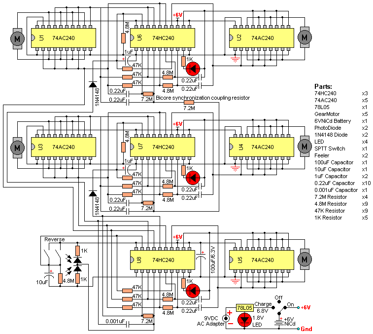
THE MOTOR DRIVERS (U1-U5) ASSEMBLY AND TESTING
The motor drivers are used to raise logic signals to sufficient power
to drive a small motor. You can use a choice of layouts to suit your needs.
One way is to assemble each motor driver on it's own separate little
board. These boards can be stacked up six modules high , plugged
like SIMMs into connectors on a mother board or they can be located
where they are needed : near each motor. Or else six drivers can be
combined on one medium size board but separated from the "brains".
Or the motor drivers can be combined with all other circuits on one
large mother board. No matter what layout you chose, each motor
driver uses one IC and associated wiring which we will treat as a
functional module.
Each motor driver module has 6 wires to connect to the rest of the
circuit : GND, +V, +IN, -IN, + OUT, - OUT.
Each motor driver uses a 74AC240 inverting buffer chip (U1-U5) and
is connected as a complete h-bridge to provide bi-directional drive
current to a small permanent magnet motor. U1-U5 are wired identically
and each controls a leg motor except for U5 which controls the waist motor.
The 74AC240 chip has 8 buffers each of which has an input and output
connected to a pin. The output pins must be wired in 2 groups of 4 in
parallel connected to the two motor terminals -OUT and +OUT.
The inputs are also connected in parallel in 2 groups of 4 (-IN and +IN)
and will be connected to the outputs of bicore circuits in U6-8.
Wire U1 as shown in the U1 layout drawing and once tested and working
you will have no problem with U2-U5 which are after all identical to U1.
These instructions asume you are prototyping but soldering the circuit
follows the same procedure. One note of caution: DO NOT CONNECT
THE BATTERY when the text refers to connecting to the power supply
terminals unless it specifically mentions BATTERY TERMINALS.
1. Lay out the location for the six external wires: motor terminals
(+OUT / -OUT) , input terminals (+IN / -IN), battery +V and GND
connections along the edges of the board.
2. Connect a wire from GND to pin 10 then to pin 1 and pin 19.
3. Connect a wire from +V to pin 20
4. Connect wires between pin 2 , 4, 6, 8 and +IN
5. Connect wires between pin 11,13,15,17 and -IN
6. Connect wires between pin 3,5,7,9,and -OUT
7. Connect wires between pin 12,14,16,18 +OUT
8. Connect a 47K resistor between pin 2 and +V (temporary)
9. Connect a 47K resistor between pin 17 and +V (temporary)
You can test each motor driver after you finish connections with
a small dc motor between pin 3 and pin 18. Connect the + and
- battery terminals to +V and GND to power up the chip. To make
the motor turn one way connect pin 2 to pin 1 (GND). To reverse
the motor remove the jumper from pin 2 to GND and connect pin
17 to GND. When pin 2 and 17 are both GND or both +V, the motor
is stopped and the "brake" is on. Try spinning the shaft of the motor
and compare with an unconnected motor. If the circuit does not work,
check your wiring. It is a simple circuit so not much can go wrong.
You can use the logic probe to confirm the +V and GND logic levels
at the outputs. Also check the motor by directly connecting it across
the battery to see if it is working. Then with an ohm meter to make
sure it is at least 30 ohms which is the probably the minimum
resisitance for use with these motor drivers. The temporary 47K
resistors can be left in for future testing or can be remeoved.
PHOTO COMPARATOR / WAIST CONTROLLER (U8)
ASSEMBLY AND TESTING
U8 is the most complicated module of the P5v2 circuit and consists
of 3 subsystem: a PD comparator, a reverser and a slave bicore for
controlling the waist motor.
A total of 10 external signals connect this chip to the rest of the cicruit:
GND, +V,PDIN,+PDC,-PDC, +IN,-IN,+OUT,-OUT, REVIN. Identify the
location of these terminal points on the edge of the board
THE U8 PHOTO COMPARATOR
The Photo Diode Comparator (PDC) is a common subsystem controlling
U6 and U7. Depending on one of three conditions the PDC reverses the
phasing of the slave bicores in U6 or U7.
The PhotoDiodes (PDs) are connected in series across the power supply
with the cathode to +V and anode to -V. This makes the PDs a light
sensitive voltage divider. The voltage at the midpoint should be +V/2
when the light is balanced on both PDs. The PD midpoint is connected
to pin 2 which is the input to the first stage of an oscillator. When the PD
midpoint is at +V/2, the oscillator generates two complementary square
waves at pin 18 and pin 16. These outputs are connected through diodes
to U6 and U7 pin 19 to control the reverser circuits of those chips.
As long as the light is balanced, the square wave will keep the 1uF
capacitors at U6/7 pin 19 positive (high) and disable the reverser of U6
and U7. When the PDs are unbalanced, the outputs of U8 pin 16 and pin
18 go one high/one low. Depending of which PD is illuminated the
brightest one of the two outputs is low which enables the control pin
19 of U6 or U7 and enables that chip's reverser subsystem.
WIRING THE PDC
The power supply connections for U8 are common for all subsystems
and are done first. Because "floating" input leads can cause problems
we will install some temporary jumpers which are later removed.
One note of caution: DO NOT CONNECT THE BATTERY when the
text refers to connecting to the power supply terminals unless it
specifically mentions BATTERY TERMINALS.
1. Connect GND to pin 10 and pin 1
2. Connect +V to pin 20,13,11 and with temporary jumpers +V to pin
15, 17, 19
3. Next we connect two PDs in series with two 1K resistors across
the power supply lead +V and GND. You must use the right polarity,
so first identify the legs of the PD to the standard diode symbol and
install with the "arrow" of the pointing to the +V side.
4. Now connect the midpoint of the two PDs (PDIN) to pin 2
5. connect a wire between pin 4 and pin 18 and +PDC (which normally
connects via diode to U6-pin19)
6. install a 7.2M resistor between pin 2 and pin 4
7. connect a 100pf-1000pf capacitor between pin 2 and pin 16
8. Connect Pin 16 to -PDC (normally connects via a diode to U7-pin 19)
9. Connect 4.8M resistor between pin 3 and pin 6 (part of slave bicore)
10. Connect a 4.8M resistor between pin 5 and pin 8 (part of slave bicore)
TESTING THE PDC
Connect the + and - battery terminals to +V and GND to power up the
chip. To check out this circuit, connect the probe alternately to pin 16
(-PDC) and pin 18 (+PDC). When the PDs are balanced (or completely
dark), the probe shines at half brightness in yellow indicating fluctuating
output signals . When one PD is much brighter than the other, the
corresponding outputs will indicate bright red or green on the probe.
Change the light to the other PD and the check the output pins and the
probe will show reversed colors. If it does not work, disconnect the PD
midpoint from the oscillator input and the LED should yellow at half
brightness. OK? ground pin 2 and LED goes either bright red or green.
OK? Connect pin 2 to +V and the LED should show reverse color on pin
16 and 18. OK. If this works it indicates a problem with the polarity of the
PDs. Swap PDs around until the outputs repond to changes in the PD
light balance. The diodes can now be installed that will connect pin 16
and 18 to U6 and U7 pin 19.
Remove battery power!
THE U8 PHASE REVERSER
The second subsystem of U8 is the phase reverser (PR) circuit which has
two inputs (pins 17/15) that are normally connected to U6-pin 16 and
U7-pin 16 . It also has two outputs (pin 3 and 5) that connect directly to
the input resistors of the U8 Slave Bicore described later.
The reverser is controlled by the voltage on U8 pin 19 which controls
whether the input signals at pin 3 and pin 5 are inverted (through the
inverter) or non-inverted (through the 47K resistors). The signals through
the reverser are normally inverted. The reverser is disabled (non-inverting)
with a +V level to pin 19 through one of the front collision switches. These
tactile sensor are also called reverser switches : There can be one switch
as a front bumper mounted on the front of the body of the walker or two
switches, one mounted on each of the front legs. These two switches
are connected in parallel. If either of the switches operates, the walker
reverses. The normally open switch contacts are connected between pin
20 (+V) and pin 19 of U8.The reverser also controls the red LED at pin 9
and applies a 47K feedback resistor to pin 19 which ensures rapid
switching when the voltage on the 10uF cap drops below +V/2. The red
LED is normally on and pulses at the same rate as the U8 slave bicore
providing a diagnostic signal.
WIRING THE U8 PHASE REVERSER
Locate the required external signals +IN and -IN from U6 and U7 pin 16
and an active high switch contact control signal REVIN at U8 pin 19 and
remove the temporary jumper from +V to pin 19.
1. Connect a wire from pin 17 to +IN
2. Connect a wire from pin 15 to -IN
3. Connect a 47K resistor from pin 3 to pin 17
4. Connect a 47K resistor from pin 5 to pin 15
5. Connect a 47K resistor from pin 7 to pin 19
6. Connect a 10uF capacitor from pin 19 to GND (polarity)
7. Connect a 4.8M resistor from pin 19 to GND
8. Connect a switch between +V and pin 19 (REVIN)
8. Connect a LED and 1K resistor in series between pin 9 and 12 (polarity)
TESTING THE U8 PHASE REVERSER
The temporary connection from +V to U8-pin 15 and 17 will be used for
testing. These temporary connections are also used to test the slave bicore.
Connect the + and - battery terminals to +V and GND. Power up and the
red LED on pin 9 will turn on. With the logic probe, check that pin 3 and 5
are both GND (green LED on). Momentarily close the reverse switch and
the red LED on pin 9 turns off for 30 seconds and then comes on again.
When the red LED is off the signal at pin 3 and 5 can not be measured with
the simple logic probe. Instead we can check the signals at the slave bicore
output pin 12 and pin 14 which are an inverted buffered version of the
reverser output signals. Those two pins should now show as GND on the
probe LED. Thirty seconds or so after momentary closing of REVIN switch pin
12 and 14 should return to +V as shown on the red probe LED.
Remove battery power!
THE U8 SLAVE BICORE
The slave Bicore input resistors (4.8M) at U8 pin 6/8 are already connected
to the reverser outputs (pin 3/5). The phase reverser normally receives
signals at +IN and -IN from U6 and U7. The slave bicore follows these
input signals but with a delay caused by the .22 uF capacitors and 4.8M
resistors. The slave bicore outputs at pin 12 and 14 normally connect to
the inputs of the waist motor driver U5.
WIRING THE U8 SLAVE BICORE
The slave bicore is practically ready and just requires two capcitors to
complete.
1. connect a 0.22uF capacitor between pin 6 and pin 12
2. connect a 0.22uF capacitor between pin 8 and pin 14
TESTING THE U8 SLAVE BICORE
Connect the + and - battery terminals to +V and GND and power up.
Since the slave bicore normally follows the alternating signals passing
through the phase reverser from U6 pin 16 and U7 pin 16. Without these
signals, the slave bicore does not work. In order to test the slave bicore
it can be made to function as a master bicore by connecting both 4.8M
resistors to GND. This is already accomplished through the reverser
which was tested earlier. The reverser inputs at pin 15 and 17 were
already connected to +V and the reverser outputs (pin 3 and 5) are
therefore at GND. Now when powered up, the slave bicore will
oscillate and the red LED at pin 9 will flash. If the reverse switch is
closed, the red LED will be off. Use the logic probe to observe the
alternating red and green LED logic states at pin 12 and 14. If U5 is
ready, then U8 pin 12 and 14 (+OUT and -OUT) can now be connected
to the U5 motor driver pin 2 and pin 11 (+IN and -IN) , and a small motor
connected to the motor driver outputs (pin 3 and pin 18) should run
alternating clockwise and counterclock wise.
This concludes the wiring and testing of U8 and the final parts of the P5v2
walker U6 and U7 are next.
THE LEG MOTOR CONTROLLERS (U6 and U7)
U6 and U7 are both wired the same way and are similar but not quite as
complex as U8. We'll refer to U6 in this text but the information applies
equally to U7.
U6 is the central pattern generator chip of the P5v2 circuit and consist
of 3 subsystem: a Master Bicore controlling the front leg motor driver, a
phase reverser and a Slave Bicore for controlling the rear leg motor driver.
A total of 9 external signals connect this chip to the rest of the cicruit:
GND, +V, +IM, -IM,+OM,-OM,+OS,-OS and REVIN. Identify the location
of these terminal points on the edge of the board
THE U6 MASTER BICORE
The master bicore (atributed to Mark Tilden of LANL) is a simple looking
oscillator with some unusual behaviour and some unusual benefits. It is
by no means the most stable oscillator and it's time constant is quite
sensitive to conducted noise. It utilizes this sensitivity toprovide
feedback
from the motor to the controller which then changes frequency in response
to mechanical loading of the motor. The feedback is not precise nor
carefully controlled but can lead to surprisingly complex behaviour
including adaptive gaits and reponse to obstacles. The bicore is a
relaxation oscillator with trigger thresholds at the end of the exponential
RC charging curve. This makes the bicore oscillation frequency low in
relation to the RC component values 0.3Hz -1Hz.
The outputs of the bicore are complementary and connect to a motor
driver chip to cause a reciprocating movement of the gear motor shaft
and a swing motion in the P5 walker legs attached to the motor shaft.
WIRING THE MASTER BICORE
The power supply connections for U6 are common for all subsystems
and are done first. Because "floating" input leads can cause problems
we will also install some other connections at this time. One note of
caution: DO NOT CONNECT THE BATTERY when the text refers to
connecting to the power supply terminals unless it specifically
mentions BATTERY TERMINALS.
1. Connect GND to pin 10 and pin 1
2. Connect +V to pin 20 , pin 11 and pin 13
3. Connect a wire between pin 15, pin 16 and -OM (later to U1 driver)
4. Connect a wire between pin 17, pin 18 and +OM (later on to U1 driver)
5. Install a 7.2M resistor between pin 2 and pin 4
6. Connect a 0.22uF capacitor between pin 2 and pin 16
7. Connect a 0.22uF capacitor between pin 4 and pin 18
8. Connect a 4.8M resistor between pin 19 and GND (part of reverser)
9. Connect a 1uF capacitor between pin 10 and GND (polarity)
10. Connect Pin 19 to REVIN normally connects via a diode to U8-pin 18)
11. Connect a 4.8M resistor between pin 3 and pin 6 (part of slave bicore)
12. Connect a 4.8M resistor between pin 5 and pin 8 (part of slave bicore)
TESTING THE U6 MASTER BICORE
Connect the + and - battery terminals to +V and GND to power up the chip.
To check out this circuit, connect the logic probe alternately to pin 16 (-OM)
and pin 18 (+OM). On each pin the logic LED flashes between red and
green about once per second.The reverser inputs at pin 15 and 17 were
already connected to pin 16 and 18 and the reverser outputs (pin 3 and 5)
are therefore the inverted function of pin 16 and 18. Use the logic probe to
confirm flasing red/green signals at pin 3 and pin 5.
The slave bicore is also connected through the 4.8M resistors it's ouputs
at pin 12 and 14 will oscillate and the red LED at pin 9 will flash. If a
momentary +V signal is applied to pin 19, the red LED will be off. Use the
logic probe to observe the alternating red and green LED logic states at
pin 12 and 14. If U1 is ready, then U6 pin 16 and 18(-OM and +OM) can
now be connected to the U1 motor driver pin 2 and pin 11 (+IN and -IN) ,
and a small motor connected to the motor driver outputs (pin 3 and pin 18)
should run alternating clockwise and counterclock wise.
Remove battery power!
THE U6 PHASE REVERSER
The second subsystem of U6 is the phase reverser (PR) circuit which has
two inputs (pins 15 and 17) that are connected to the master bicore output
signals at pin 16 and 18 It also has two outputs (pin 3 and 5) that connect
directly to the input resistors of the U6 Slave Bicore described later. The
reverser is controlled by the voltage on U6 pin 19 which controls whether
the input signals at pin 3 and pin 5 are inverted (through the inverter) or
non-inverted (through the 47K resistors). The signals through the reverser
are normally inverted. The reverser is disabled (non-inverting) with a +V
level to pin 19 through a diode from the Photo Diode Comparator circuit
on U8 (pin 18) . The reverser also controls the red LED at pin 9 and
applies a 47K feedback resistor to pin 19 which ensures rapid switching
when the voltage on the 1uF cap drops below +V/2. The red LED is normally
off and when "turning" the LED pulses at the same rate as the U6 slave
bicore providing a diagnostic signal.
WIRING THE U6 PHASE REVERSER
1. Connect a 47K resistor from pin 3 to pin 17
2. Connect a 47K resistor from pin 5 to pin 15
3. Connect a 47K resistor from pin 7 to pin 19
4. Connect a LED and 1K resistor in series between pin 9 and 12 (polarity)
TESTING THE U6 PHASE REVERSER
Connect the + and - battery terminals to +V and GND. Power up and the
red LED on pin 9 will turn on. With the logic probe, check that pin 3 and
5 are both pulsing. Apply a connection from +V to pin 19 and the red LED
on pin 9 turns off for a few seconds and then comes on again. When the
red LED is off the signal at pin 3 and 5 can not be measured with the
simple logic probe. Instead we can check the signals at the slave bicore
output pin 12 and pin 14 which are an inverted buffered version of the
reverser output signals. Those two pins should both show the slow
oscillating signal of the master bicore. A few seconds after the
momentary application of +V tothe REVIN (pin 19) the phasing of pin
12 and 14 will switch but both continue to oscillate.
Remove battery power!
THE U6 SLAVE BICORE
The slave Bicore input resistors (4.8M) at U8 pin 6/8 are already
connected to the reverser outputs (pin 3/5). The phase reverser
passes the signals from the master bicore straight through or
phase inverted. The slave bicore follows these input signals but
with a delay caused by the .22 uF capacitors and 4.8M resistors.
The slave bicore outputs at pin 12 and 14 normally connect to the
inputs of the motor driver U2.
WIRING THE U6 SLAVE BICORE
The slave bicore is practically ready and just requires two capcitors
to complete.
1. connect a 0.22uF capacitor between pin 6 and pin 12
2. connect a 0.22uF capacitor between pin 8 and pin 14
TESTING THE U6 SLAVE BICORE
Connect the + and - battery terminals to +V and GND and power up.
Since the slave bicore normally follows the alternating signals passing
through the phase reverser from U6 pin 16 and U7 pin 16. With these
signals, the slave bicore will oscillate with a time delay with respect to
the master bicore and the red LED at pin 9 will flash at the slave bicore
rate. If the +V signal is applied to pin 10 (REVIN), the red LED will be
off. Use the logic probe to observe the alternating red and green LED
logic states at pin 12 and 14. If U2 is ready, then U6 pin 12 and 14
(+OUT and -OUT) can now be connected to the U2 motor driver pin 2
and pin 11 (+IN and -IN) , and a small motor connected to the motor
driver outputs (pin 3 and pin 18) should run alternating clockwise and
counterclock wise.
THE P5v2 FINAL CIRCUIT ASSEMBLY
The previous sections provided a step by step assembly and debugging
procedure for each type of functional module using U1, U6 and U8 as
examples.
To complete the circuit these instructions can be used to also assemble
and test motor drivers U2-U5. In addition U7 must be assembled and
tested the same way as U6. Then comes the part of integrating these
functional block. and the mecahnical assembly of tho walker including
the motor placement and leg attachement as well as mounting the
sensors. The schematic and layout drawing will help you in making the
required connections between the functional blocks and the motors. In
particular, connect each block one at a time and test functionality. One
final note, remember to connect the phase synchronizing 7.2M resistor
between pin 2 of U6 and U7. Also be sure to add the diodes between
U8 pin 16 and U6 pin 19 and U8 pin 18 and U7 pin 19. I will soon provide
a series of photos showing the progress of building the P5v2 Walker to
ilustrate the text.
Notes:
The 100uF capacitor is connected across the powersupply to provide
filtering of any noise from the motors from interfering with the
electronics.
Not shown are optional 0.1 uF ceramic caps between pin 10 and 20.
They are not always needed : it depends on the motors and battery you
use. Beam circuit depend somewhat on coupled motor noise to provide
feedback to the electronics. This feedback is an imprecise art, using
increased motor noise to shorten the period of the oscillators to change
the gait especially when the motors are struggling from heavy mechanical
loading. If you added the caps it may slow the oscillation and remove this
valuable feedback . If circuit operation is eratic because of coupled
motor noise you can add those capacitors.
wilf
|